iMX8MM SBC Extends HDMI and LVDS Display
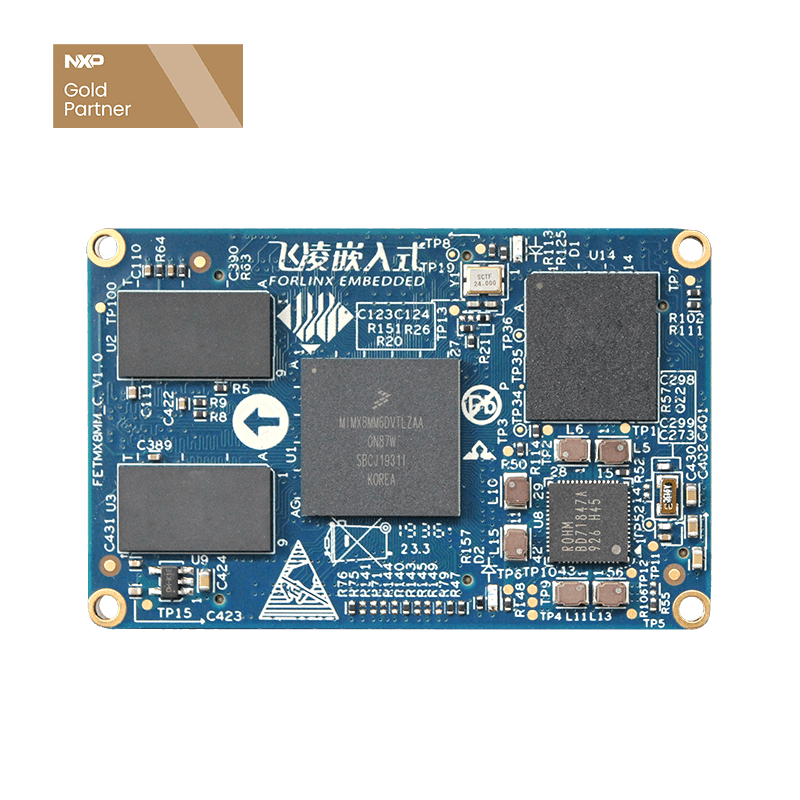
FETMX8MM-C SoM is based on NXP's iMX8M Mini quad-core 64-bit processor design with a main frequency of up to 1.8GHz, Cortex-A53 architecture, and 2GB DDR4 RAM for a universal Cortex®-M4 400MHz core processor. A variety of audio interfaces are available, including I2S, AC97, TDM, PDM, and SPDIF. A variety of peripheral interfaces are available, such as MIPI-CSI, MIPI-DSI, USB, PCIe, UART, eCSPI, IIC, and Gigabit Ethernet.
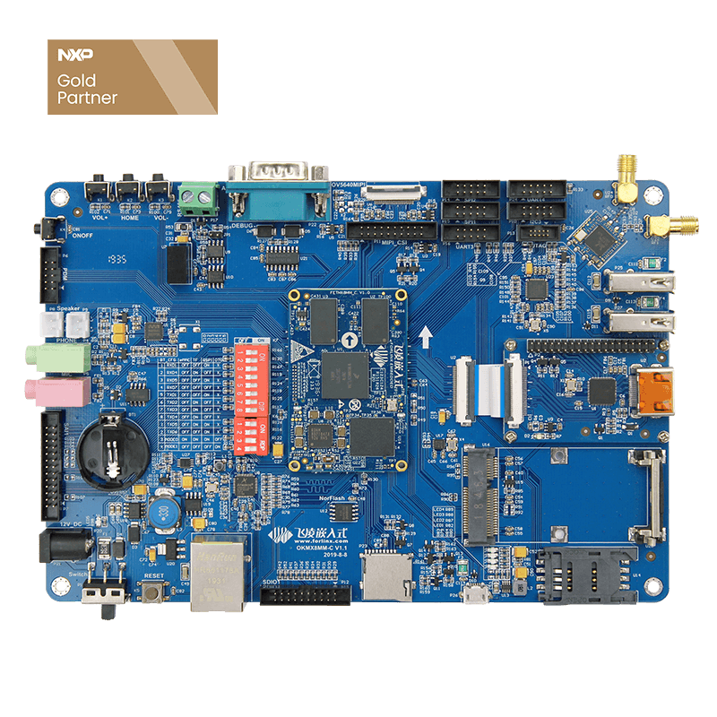
Forlinx iMX8MM core board has an H.265 and VP9 decoder at 1080p 60Hz; Compared with the traditional H.264 encoding, the average decoding efficiency is 50%; The bandwidth and capacity of transmitting and storing video at the same resolution is 50% of H.264. In order to facilitate customers to evaluate iMX8M mini processor performance, core board stability, OKMX8MM-C development board led to a wide variety of interfaces complete, reasonable layout.
OKMX8MM-C development board only supports all the way MIPI_DSI display interface, in order to enrich the iMX8 series of product display interface resources, Forlinx embedded for iMX8MM product development supporting display transfer module FIT-HDMI -LVDS-I, can achieve the MIPI_DSI display signal into HDMI and LVDS display, and support HDMI and LVDS display.
The MIPI interface uses a 30pin FPC socket, the LVDS interface uses a 2mm pitch pin lead, and HDMI uses a standard Type A interface. The FIT-HDMI-LVDS-I module master chip uses Longxun Semiconductor LT8912B, LT8912B has a single MIPI D-PHY receiver, has 4 data channels, each data channel at 80Mbps to 1.5Gbps speed, the maximum input bandwidth is 6Gbps. The LVDS has 1 clock lane and 4 data lanes, with a maximum of 1.0Gbps per data channel. HDMI output supports HDMI 1.4 and up to 60Hz 1080p 8-bits output. The LT8912B does not support DDC and HDCP.
As the information of Longxun LT8912B chip is not disclosed, the small editor here for you to briefly introduce, based on The Forlinx embedded iMX8MM product extension HDMI and LVDS display, the development process of hardware design needs to pay attention to the pit.
- 1.LT8912B chip only needs 1.8V power supply, but the chip is divided into many power domains, each way need to use separate magnetic beads and capacitive filtering.
- 2. The IO pins of the chip, such as the IIC, RST, INT and HDMI HPD pins, are all 1.8V levels, and when connected to other MCUs, please note their level status, need to do level conversion.
- 3. In the principle provided by Forlinx embedded, there are two GPIO made a compatible design, can do LT8912B reset and interrupt, but also can connect the LVDS screen touch chip reset and interrupt. After practical testing, the LT8912B reset and interrupt signals do not have to be controlled by GPIO, so Forlinx embedded designers assigned these two GPOS to the LVDS touch screen. The reset of the LT8912B is available using an RC reset.
- 4. Since the data channel of this chip is high-speed signal, it is highly recommended to use the 4-layer board design, and pay attention to the impedance matching of the differential pair 100 s±10%, the difference between the pairs, the difference between the groups need to do so long.
- 5. The maximum current of the chip is about 5V/300mA, and the heat is not very large.
The following is the schematic of the HDMI-LVDS transfer module, hoping to help you in the product design.


