Application of i.MX RT1052 Core Board in Automotive Diagnostic Equipment
First, industry background
At present, the traditional automotive programmers on the market are designed for specific automobile manufacturers IC, can not be compatible with other manufacturers IC, communication schemes with the upper computer, most of the use of traditional serial communication; Single power supply, can not meet the needs of subsequent expansion; The master chip is still stuck in the 8-bit microcontroller stage, its processing speed can not meet customer demand, the programmer pin level can only be compatible with 5V. With the diversification of automotive ICs, a wide variety of automotive IC programmers have emerged, making their use more complex for customers.
Second, technical parameters
- 1, High-speed USB 2.0 communication
- 2, Flexible programming pin function
- 3, A variety of vehicle and vehicle equipment data diagnostic interface (LIN, K, CAN)
- 4, High-speed processing speed
- 5, High equipment safety performance
- 6, Large-capacity storage
- 7, Reserved application processor function (subsequent expansion of the operating system)
Third, recommend the program
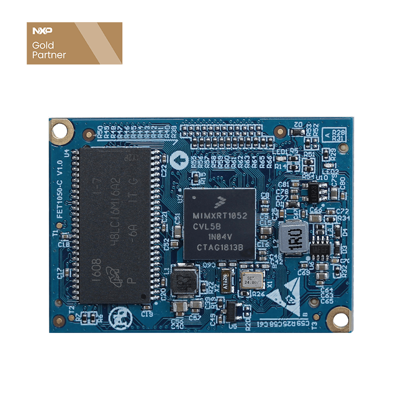
The FET1052-C is based on the Arm® Cortex ®-M7 core, i.MXRT1052 crossover processor design, operating at 528 MHz. Up to 512KB tightly coupled memory (TCM), real-time low latency response, as low as 20ns, perfectly combines the high performance, scalability, and low power consumption, high real-time, and easy-to-develop benefits of application processors.
FET1052-C SoM Front Side
FET1052-C SoM Rear Side
FET1052-C SoM Size
1.RT1052 SoM configuration resources
| Configure 1 | Configure 2 |
| Main frequency: 528MHz operating ambient temperature: -40℃to 85℃ | Main Frequency: 528MHz Operating ambient temperature: -40℃ to 85℃ |
| SDRAM: 32MB | SDRAM: 16MB |
| ROM: 16MB QSPI-NOR Flash | ROM:4MB QSPI-NOR Flash |
2.RT10532 SoM interface resources:
Fourth, the implementation of the program
- 1. High-speed USB communication
- 2. Flexible programming pin function reuse
- 3.A variety of vehicle and on-board equipment data diagnostic interface
- 4. High-speed processing and running speed
- 5. High equipment safety performance
- 6. Large storage capacity
FET1052-C supports high-speed USB 2.0 mode with an interface speed of 480Mbps. Fully meets speed requirements. At the same time can be external USB HUB chip, easy for users to expand.
FET1052-C interface is rich in resources, such as UART, IIC, SPI and other common programming communication protocols are introduced.
Supports 2-Lane CAN for data communication with on-board controllers or other on-board equipment. FET1052-C supports up to 8 UARTS, each with a maximum support of 5.0 Mbps, and the K and LIN interfaces are easily implemented via an extended conversion chip.
The i.MX RT1052 operates at 600 MHz (528MHz in industrial class) based on the Arm ® Cortex ®-M7 core. Up to 512KB tightly coupled memory (TCM), real-time low latency response as low as 20 ns. This is perfectly sufficient.
The FET1052-C cross-border processor solution uses hardware-accelerated encryption modules that enable data to be stored in encrypted format in external memory. Encrypted data is transferred to the chip when needed and decrypted "instantly" at read time, without the need for a cycle of waiting to be decrypted. These advanced encryption accelerators in cross-border processors significantly increase encryption/decryption throughput, eliminating the need for on-chip non-volatile memory for security. High-performance cores for cross-border processors can be used to implement software encryption, even when hardware encryption is not applicable. This is a clear advantage over traditional MCUs.
Ideally, embedded processors perform the highest performance when executable code and data are stored in in-chip SRAM and CPU core operations are performed from this storage. Even in in-chip SRAM, only TightLy Coupled Memory (TCM) provides single-cycle access to the core. Access to any memory other than TCM increases the required CPU clock cycle, with increasing access losses from level 2 cache to in-chip flash to external flash. Because of the application processor architecture, cross-border processors can be manufactured on advanced technology nodes (40nm and higher) with significantly reduced SRAM bit units, making integrating high-density SRAM more cost-effective than embedding flash memory. In a cross-border design architecture, SRAM can be configured to have a "zero wait" single-cycle access TCM, significantly improving system performance. With this critical design feature, cross-border processors will be far more effective than their MCU equivalents. Easy to expand memory chips, such as external expansion SDRAM, flash, etc.


